Intel is an old stalwart of the computing industry founded in 1968. In fact Intel is older than I am. They made the first microprocessor in 1971. Today Intel has over 99000 employees, 199 offices and facilities, 38.8 Billion in revenue and is number 50 in the Fortune 500. The first computer I ever bought was based upon a 286-12 with 1MB of memory, a 20MB hdd and a 10 inch monitor.
Over the years I’ve had many systems with Intel CPUs and chipset. The first modern system I built had a Intel Pentium 120 with 8MB of memory, a Trident 1MB 8900 ISA video card and a 1GB HDD. The second Intel-based computer I built was a 300MHz Pentium II Klamath with 128MB of memory, 20GB HDD and an ATI Rage Pro Turbo video card.
Intel really was the enthusiast’s only choice for years. Sure Apple had its day, and eventually AMD got into the picture (today AMD and Intel are virtually tied for market share in the retail market). AMD has had a leg up on Intel for the last few years in the enthusiast market, with the introduction of the Athlon 64, the dual core Athlon 64s X2 and more.
One of the big problems with Intel in recent years has been their CPUs run so hot at times with standard cooling that they would give heat errors on boot. The first Prescott CPU that Intel sent for evaluation purposes would not even boot on three MSI motherboards that ran other Intel CPUs 100% fine. Our 955 evaluation CPU runs so hot that I shudder to think of it running every day.
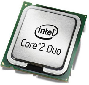
Intel introduced their first LGA-775 Prescott and Extreme Edition processors in 2004 along with the 925X and 915 chipset platforms. Subsequent processors have included the 6xx series (adding 64-bit instruction support), the 8xx series (Dual core), and the 9xx series (4MB L2 cache instead of 2MB on the 8xx series). Today Intel is announcing their next iteration of their CPU architecture, the Intel Core 2 Duo processors and the 965 chipset.
The New CPU Details
| Processor number | Frequency | FSB | L2 Cache | Price July 23 |
| C2D X6800 | 2.93 GHz | 1066MHz | 4MB | $999 |
| C2D E6700 | 2.67 GHz | 1066MHz | 4MB | $530 |
| C2D E6600 | 2.4 GHz | 1066MHz | 4MB | $316 |
| C2D E6400 | 2.13 GHz | 1066MHz | 2MB | $224 |
| C2D E6300 | 1.86 GHz | 1066MHz | 2MB | $183 |
| P4D 945 | 3.4 GHz | 800MHz | 2×2 MB | $163 |
| P4D 915 | 2.8 GHz | 800MHz | 2x2MB | $133 |
| P4D 820 | 2.8 GHz | 800MHz | 2×1 MB | $113 |
| P4D 805 | 2.66GHz | 533MHz | 2x1MB | $93 |
Intel’s processor architecture has its roots based in the x86 architecture they introduced way back in 1981. They’ve increased the clock speed, increased the L1 cache, improved the L2 cache, added MultiMedia eXtensions, SSE1-3 instructions, 64-bit instructions, dual cores on a single die and more to make today’s Core 2 Duo CPUs, but the basic core is still on the x86 architecture.
Intel’s new CPUs are based upon a 65 nanometer process, the same process as the earlier CPUs. Intel is at the forefront of process technology with 45 nanometer products coming out in the next year. AMD is still on the 90 nanometer node, meaning Intel has the room to put more transistors, and more cache on the same die area for less power consumption.
Intel has finally changed the naming scheme of their CPUs. The name Pentium has been around since 1995, and is getting old, like NVIDIA’s GeForce or AMD’s Athlon name. It’s been for a long time that companies should use of that vast advertising budget they have and think of, and market new names every once in a while. Intel introduced the Core name with their mobile CPUs earlier this year. The new desktop CPUs are called Core 2 Duo and Core 2 Extreme. Let’s take a quick look at the Netburst architecture.
The Pentium 4 line of CPUs were the first CPUs based upon the Netburst Microarchitecture. Netburst had features like Hyper Pipelining, a Rapid Execution Engine, and a Execution Trace Cache. Hyper Pipelined technology was Intel’s name for the 20 stage pipeline on the original Pentium 4 CPUs. Prescott CPUs had a 31 stage pipeline. More stages meant fewer instructions per cycle, but allowed for a higher clock speed. This allowed Intel to release 3.8GHz CPUs while AMD was stuck on a 2.4GHz clock speed for a long time. The rapid execution engine means that the ALU or computational units is clocked at twice the CPU’s clock speed. Execution Trace Cache stores decoded micro-operations, so that when the CPU executes a new instruction the decoded micro-op can be read from the Execution Trace Cache instead of fetching and decoding the instruction again.
The new Core 2 CPUs have Wide Dynamic Execution. Each of the Core 2 Duo’s cores can execute up to four full instructions simultaneously in a 14-stage pipeline, less than ½ that of the Prescott CPUs of the last architecture. The previous generation could execute a maximum of 3 full CPU instructions per core in a cycle. When combined with a deeper pipeline, the Prescott CPUs were slower clock for clock than the previous architecture. So clock for clock the Core 2 CPUs should be much faster than any Netburst CPU.
The amount of cache on a CPU is important to performance. The Core 2 Duo and Extreme CPUs have 32KB of L1 cache. They also have 4MB of unified L2 cache. This means that the L2 cache is shared by the two cores. AMD’s X2 CPUs are non-unified, in that each CPU core has its own L2 cache. If the same data is required for multiple cores the data need only be stored once, while on a non-unified L2 cache a copy is shared on each core’s cache. Intel calls this Intel Advanced Smart Cache.
The last new feature of Intel’s new architecture is called Intel Advanced Digital Media Boost. Streaming SIMD Extensions are accelerated to one 128-bit instruction per clock cycle with the Core 2 CPUs; double that of the previous generation. SSE, SSE2, SSE3 instructions are supported as well as the Extended Memory 64 Technology introduced with Intel’s 6xx series of CPUs.
Today Intel has provided me with two CPUs to review, the Core 2 Extreme X6800 and the Core 2 Duo E6700 CPU. The X6800 is clocked a 2.93GHz, slower in clock speed than the fastest dual core CPUs, but speed isn’t everything as any owner of an AMD Athlon 64 CPU would attest to. The E6700 is clocked at a more modest 2.66GHz, 10% slower in pure clock speed. It’ll be interesting to see how performance will factor into the CPU.
The other CPUs in the lineup are interesting and analogues to the lineup previous to the Core 2 launch. The E6600 is slightly lower clocked than the E6700. The 6400 and 6300 have half the unified L2 cache of the X6800 and E6700 and are lower clocked as well. The 945 and 915 are Dual Core CPUs based on the Netburst micro-architecture. Note the L2 cache on NetBurst CPUs is 2MB per core, not one 4MB cache. The 820 and 815 CPUs have two 1MB caches.
Also Read: Top Pick Motherboard For Ryzen 5 5600X
